

On 24 July 2026, our Faculty of Engineering’s Department of Materials Engineering had the opportunity to welcome Dr Thanet Pakpuwadon (MatE16, E69, KU73), an alumnus of the department who is affectionately known as “P’Ou”. Dr Thanet is currently a Layout Design Engineer at Micron Technology in Japan. He designs DRAM and CMOS chip circuits and joined us to share his professional experience, career journey, and inspiration with students in the fields of Semiconductor Engineering and Materials Engineering.
Micron Technology is one of the world’s leading memory semiconductor companies and among the largest memory chip manufacturers globally, alongside Samsung Electronics and SK Hynix. This talk therefore offered students a valuable perspective from someone working directly in the forefront of the semiconductor industry.

During the session, students learned about:
- An overview of careers in the semiconductor industry, particularly the memory production chain — from design through manufacturing
- The work of semiconductor engineers in Japan
- Salaries, benefits, and career-growth opportunities
- The working environment and culture at Micron Technology Japan
The session was filled with knowledge-sharing and thoughtful questions from students. It gave them a clearer picture of career paths in the semiconductor industry and helped inspire their aspirations to become internationally competitive semiconductor engineers.
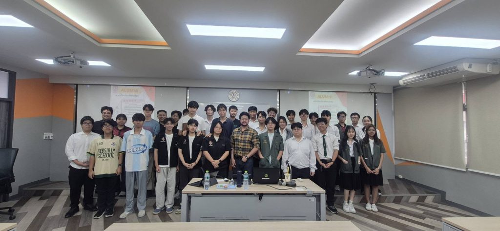


The department sincerely thanks Dr Thanet for taking time during his vacation to return to his alma mater and share his knowledge, experience, and insights from working at a global semiconductor company. We believe that today’s experience will encourage students to move confidently towards their futures in the semiconductor industry.
The best inspiration comes from learning from those who are already doing what we aspire to achieve.

